A premier value-added metal service center
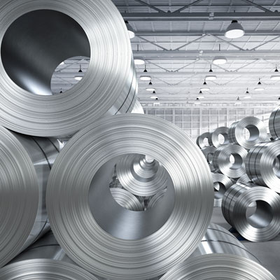
Wieland Metal Services’ selection of metal products is among the most extensive in the industry today. The inventory includes a full range of copper and copper-based alloys, aluminum and stainless steel in various forms including extrusions, foil, plate, rod, bar, wire, tube, sheet, and strip/coil.
At Wieland Metal Services, the pursuit of continuous quality improvement defines our corporate culture from top to bottom allowing us to provide the finest quality metal products and services in response to each customer’s specific needs.
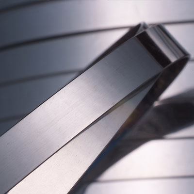
Aluminum
We offer aluminum sheet and foil gauges in a wide variety of alloys, tempers, and finishes.

Copper & Copper Alloys
We stock and supply the broadest product range of copper and brass alloys in the industry.
Stainless Steel
We offer a wide range of stainless steel alloys in both foil and sheet gauges.

Architectural Copper
We offer copper roofing products, including copper roofing sheet and coil, lead-coated copper and tin-zinc coated copper.
Value proposition
Wieland Metal Services continually works toward improving processes and educating employees to help create a safer and more productive workplace. Relying on these core values, provides high-quality products and reliable services for our customers.
With a base attitude to be better tomorrow than today, we deliver outstanding business results each day.
- A safety-first driven company
- 100% recyclable products
- Short lead times
- Excellent customer service
- Diverse metal product offering: Copper, Brass, Aluminum, Stainless Steel
- Wide-range of processing capabilities – from .0005 to .2500 inch thickness
- Expansive geographic coverage in the US, Mexico, and Puerto Rico
- High-quality standards – ISO 9001 certified

Our Markets
Wieland Metal Services serves an extensive base of industries and have proven capable of meeting and exceeding numerous industry’s exceptionally stringent demands for product quality, deliverability, and Just-in-Time performance at every point in the supply chain. We offer stocking programs, help with logistics, and make sure to provide the correct alloy for every application. Our locations are strategically located through the US, Carribean, and Mexico to serve the needs of the industry.
Ammunition
Antimicrobial Copper
Architectural Products
Automotive
Building & Construction
Coinage
Electrical and Electronics
Energy
HVAC
Jewelry
Medical
Signage
Trailers
And many more…
About Us
Wieland Metal Services is a leading value-added metal service center in North America. As part of the Wieland Group since July 2019, Wieland Metal Services continues to focus on safety, quality and customer service. Learn more at Wieland.com
Copyright 2021 © Wieland
All Rights Reserved
Privacy Policy. Harassment Policy
Terms and Conditions
Copyright 2021 © Wieland
All Rights Reserved
Privacy Policy. Harassment Policy
Terms and Conditions